BTemplates.com

Powered by Blogger.

Pageviews past week

Quantum mechanics

Auto News

artificial intelligence

About Me

Recommend us on Google!

Information Technology

Popular Posts

Showing posts with label Graphene. Show all posts

Monday, October 10, 2011

Graphene's 'Big Mac' creates next generation of chips


The world's thinnest, strongest and most conductive material, discovered in 2004 at the University of Manchester by Professor Andre Geim and Professor Kostya Novoselov, has the potential to revolutionize material science.
Artistic impression of graphene molecules.
Image: University of Manchester

Demonstrating the remarkable properties of graphene won the two scientists the Nobel Prize for Physics last year and UK's Chancellor of the Exchequer George Osborne has just announced plans for a £50m graphene research hub to be set up.

Now, writing in the journal Nature Physics, the University of Manchester team have for the first time demonstrated how graphene inside electronic circuits will probably look like in the future.

By sandwiching two sheets of graphene with another two-dimensional material, boron nitrate, the team created the graphene 'Big Mac' – a four-layered structure which could be the key to replacing the silicon chip in computers.

Because there are two layers of graphene completed surrounded by the boron nitrate, this has allowed the researchers for the first time to observe how graphene behaves when unaffected by the environment.

Dr Leonid Ponomarenko, the leading author on the paper, said: "Creating the multilayer structure has allowed us to isolate graphene from negative influence of the environment and control graphene's electronic properties in a way it was impossible before.

"So far people have never seen graphene as an insulator unless it has been purposefully damaged, but here high-quality graphene becomes an insulator for the first time."

The two layers of boron nitrate are used not only to separate two graphene layers but also to see how graphene reacts when it is completely encapsulated by another material.

Professor Geim said: "We are constantly looking at new ways of demonstrating and improving the remarkable properties of graphene."

"Leaving the new physics we report aside, technologically important is our demonstration that graphene encapsulated within boron nitride offers the best and most advanced platform for future graphene electronics. It solves several nasty issues about graphene's stability and quality that were hanging for long time as dark clouds over the future road for graphene electronics.

We did this on a small scale but the experience shows that everything with graphene can be scaled up."

"It could be only a matter of several months before we have encapsulated graphene transistors with characteristics better than previously demonstrated."

Graphene is a novel two-dimensional material which can be seen as a monolayer of carbon atoms arranged in a hexagonal lattice.

Its remarkable properties could lead to bendy, touch screen phones and computers, lighter aircraft, wallpaper-thin HD TV sets and superfast internet connections, to name but a few.

Provided by University of Manchester

Tuesday, June 21, 2011

Scientists find simple way to produce graphene


Scientists at Northern Illinois University say they have discovered a simple method for producing high yields of graphene, a highly touted carbon nanostructure that some believe could replace silicon as the technological fabric of the future.
Amartya Chakrabarti holds up a sample of
graphene produced via the dry-ice method.
Credit: Scott Walstrom, Northern Illinois University

The focus of intense scientific research in recent years, graphene is a two-dimensional material, comprised of a single layer of carbon atoms arranged in a hexagonal lattice. It is the strongest material ever measured and has other remarkable qualities, including high electron mobility, a property that elevates its potential for use in high-speed nano-scale devices of the future.

In a June communication to the Journal of Materials Chemistry, the NIU researchers report on a new method that converts carbon dioxide directly into few-layer graphene (less than 10 atoms in thickness) by burning pure magnesium metal in dry ice.

"It is scientifically proven that burning magnesium metal in carbon dioxide produces carbon, but the formation of this carbon with few-layer graphene as the major product has neither been identified nor proven as such until our current report," said Narayan Hosmane, a professor of chemistry and biochemistry who leads the NIU research group.

"The synthetic process can be used to potentially produce few-layer graphene in large quantities," he said. "Up until now, graphene has been synthesized by various methods utilizing hazardous chemicals and tedious techniques. This new method is simple, green and cost-effective."

Hosmane said his research group initially set out to produce single-wall carbon nanotubes. "Instead, we isolated few-layer graphene," he said. "It surprised us all."

"It's a very simple technique that's been done by scientists before," added Amartya Chakrabarti, first author of the communication to the Journal of Materials Chemistry and an NIU post-doctoral research associate in chemistry and biochemistry. "But nobody actually closely examined the structure of the carbon that had been produced."


Provided by Northern Illinois University

Saturday, June 11, 2011

Engineers Envision 'Two-Dimensional' Graphene Metamaterials and One-Atom-Thick Optical Devices


Two University of Pennsylvania engineers have proposed the possibility of 'two-dimensional' metamaterials. These one-atom-thick metamaterials could be achieved by controlling the conductivity of sheets of graphene, which is a single layer of carbon atoms.
A graphene waveguide and splitter. (Credit: Image courtesy of University of Pennsylvania)

Professor Nader Engheta and graduate student Ashkan Vakil, both of the Department of Electrical and Systems Engineering in Penn's School of Engineering and Applied Science, published their theoretical research in the journal Science.

The study of metamaterials is an interdisciplinary field of science and engineering that has grown considerably in recent years. It is premised on the idea that materials can be designed so that their overall wave qualities rely not only upon the material they are made of but also on the pattern, shape and size of irregularities, known as "inclusions," or "meta-molecules" that are embedded within host media.

"By designing the properties of the inclusions, as well as their shapes and density, you achieve in the bulk property something that may be unusual and not readily available in nature," Engheta said.

These unusual properties generally have to do with manipulating electromagnetic (EM) or acoustic waves; in this case, it is EM waves in the infrared spectrum

Changing the shape, speed and direction of these kinds of waves is a subfield of metamaterials known as "transformation optics" and may find applications in everything from telecommunications to imaging to signal processing.

Engheta and Vakil's research shows how transformation optics might now be achieved using graphene, a lattice of carbon a single atom thick.

Researchers, including many at Penn, have devoted considerable effort into developing new ways to manufacture and manipulate graphene, as its unprecedented conductivity would have many applications in the field of electronics. Engheta and Vakil's interest in graphene, however, is due to its capability to transport and guide EM waves in addition to electrical charges and the fact that its conductivity can be easily altered.

Applying direct voltage to a sheet of graphene, by way of ground plate running parallel to the sheet, changes how conductive the graphene is to EM waves. Varying the voltage or the distance between the ground plate and the graphene alters the conductivity, "just like tuning a knob," Engheta said.

"This allows you to change the conductivity of different segments of a single sheet of graphene differently from each other," he said. And if you can do that, you can navigate and manipulate a wave with those segments. In other words, you can do transformation optics using graphene."

In this marriage between graphene and metamaterials, the different regions of conductivity on the effectively two-dimensional, one-atom-thick sheet function as the physical inclusions present in three-dimensional versions.

The examples Engheta and Vakil have demonstrated with computer models include a sheet of graphene with two areas that have different conductivities, one that can support a wave, and one that cannot. The boundary between the two areas acts as a wall, capable of reflecting a guided EM wave on the graphene much like one would in a three dimensional space.

Another example involves three regions, one that can support a wave surrounded by two that cannot. This produces a "waveguide," which functions like a one-atom-thick fiber optic cable. A third example builds on the waveguide, adding another non-supporting region to split the waveguide into two.


"We can 'tame' the wave so that it moves and bends however we like," Engheta said. "Rather than playing around with the boundary between two media, we're thinking about changes of conductivity across a single sheet of graphene."

Other applications include lensing and the ability to do "flatland" Fourier transforms, a fundamental aspect of signal processing that is found in nearly every piece of technology with audio or visual components.

"This will pave the way to the thinnest optical devices imaginable," Engheta said. "You can't have anything thinner than one atom!"

Support for this research came from U.S. Air Force Office of Scientific Research.

Tuesday, May 10, 2011

Optical Computing in Electronics


Scientists at the University of California, Berkeley, have demonstrated a new technology for graphene that could break the current speed limits in digital communications.
This is a schematic illustration of the graphene-based 
optical modulator. A layer of graphene (black fishnet) 
is placed on top of a silicon waveguide (blue), which 
is used as an optical fiber to guide light. Electrical 
signals are sent in from the side of the graphene to 
alter the amount of photons the graphene absorbs. 
(Credit: Graphic by Ming Liu, UC Berkeley)

The team of researchers, led by UC Berkeley engineering professor Xiang Zhang, built a tiny optical device that uses graphene, a one-atom-thick layer of crystallized carbon, to switch light on and off. This switching ability is the fundamental characteristic of a network modulator, which controls the speed at which data packets are transmitted. The faster the data pulses are sent out, the greater the volume of information that can be sent. Graphene-based modulators could soon allow consumers to stream full-length, high-definition, 3-D movies onto a smartphone in a matter of seconds, the researchers said.

"This is the world's smallest optical modulator, and the modulator in data communications is the heart of speed control," said Zhang, who directs a National Science Foundation (NSF) Nanoscale Science and Engineering Center at UC Berkeley. "Graphene enables us to make modulators that are incredibly compact and that potentially perform at speeds up to ten times faster than current technology allows. This new technology will significantly enhance our capabilities in ultrafast optical communication and computing."

In this latest work, described in the May 8 advanced online publication of the journal Nature, researchers were able to tune the graphene electrically to absorb light in wavelengths used in data communication. This advance adds yet another advantage to graphene, which has gained a reputation as a wonder material since 2004 when it was first extracted from graphite, the same element in pencil lead. That achievement earned University of Manchester scientists Andre Geim and Konstantin Novoselov the Nobel Prize in Physics last year.

Zhang worked with fellow faculty member Feng Wang, an assistant professor of physics and head of the Ultrafast Nano-Optics Group at UC Berkeley. Both Zhang and Wang are faculty scientists at Lawrence Berkeley National Laboratory's Materials Science Division.

"The impact of this technology will be far-reaching," said Wang. "In addition to high-speed operations, graphene-based modulators could lead to unconventional applications due to graphene's flexibility and ease in integration with different kinds of materials. Graphene can also be used to modulate new frequency ranges, such as mid-infrared light, that are widely used in molecular sensing."

Graphene is the thinnest, strongest crystalline material yet known. It can be stretched like rubber, and it has the added benefit of being an excellent conductor of heat and electricity. This last quality of graphene makes it a particularly attractive material for electronics.

"Graphene is compatible with silicon technology and is very cheap to make," said Ming Liu, post-doctoral researcher in Zhang's lab and co-lead author of the study. "Researchers in Korea last year have already produced 30-inch sheets of it. Moreover, very little graphene is required for use as a modulator. The graphite in a pencil can provide enough graphene to fabricate 1 billion optical modulators."

It is the behavior of photons and electrons in graphene that first caught the attention of the UC Berkeley researchers.

The researchers found that the energy of the electrons, referred to as its Fermi level, can be easily altered depending upon the voltage applied to the material. The graphene's Fermi level in turn determines if the light is absorbed or not.

When a sufficient negative voltage is applied, electrons are drawn out of the graphene and are no longer available to absorb photons. The light is "switched on" because the graphene becomes totally transparent as the photons pass through.

Graphene is also transparent at certain positive voltages because, in that situation, the electrons become packed so tightly that they cannot absorb the photons.

The researchers found a sweet spot in the middle where there is just enough voltage applied so the electrons can prevent the photons from passing, effectively switching the light "off."

"If graphene were a hallway, and electrons were people, you could say that, when the hall is empty, there's no one around to stop the photons," said Xiaobo Yin, co-lead author of the Nature paper and a research scientist in Zhang's lab. "In the other extreme, when the hall is too crowded, people can't move and are ineffective in blocking the photons. It's in between these two scenarios that the electrons are allowed to interact with and absorb the photons, and the graphene becomes opaque."

In their experiment, the researchers layered graphene on top of a silicon waveguide to fabricate optical modulators. The researchers were able to achieve a modulation speed of 1 gigahertz, but they noted that the speed could theoretically reach as high as 500 gigahertz for a single modulator.

While components based upon optics have many advantages over those that use electricity, including the ability to carry denser packets of data more quickly, attempts to create optical interconnects that fit neatly onto a computer chip have been hampered by the relatively large amount of space required in photonics.

Light waves are less agile in tight spaces than their electrical counterparts, the researchers noted, so photon-based applications have been primarily confined to large-scale devices, such as fiber optic lines.

"Electrons can easily make an L-shaped turn because the wavelengths in which they operate are small," said Zhang. "Light wavelengths are generally bigger, so they need more space to maneuver. It's like turning a long, stretch limo instead of a motorcycle around a corner. That's why optics require bulky mirrors to control their movements. Scaling down the optical device also makes it faster because the single atomic layer of graphene can significantly reduce the capacitance -- the ability to hold an electric charge -- which often hinders device speed."

Graphene-based modulators could overcome the space barrier of optical devices, the researchers said. They successfully shrunk a graphene-based optical modulator down to a relatively tiny 25 square microns, a size roughly 400 times smaller than a human hair. The footprint of a typical commercial modulator can be as large as a few square millimeters.

Even at such a small size, graphene packs a punch in bandwidth capability. Graphene can absorb a broad spectrum of light, ranging over thousands of nanometers from ultraviolet to infrared wavelengths. This allows graphene to carry more data than current state-of-the-art modulators, which operate at a bandwidth of up to 10 nanometers, the researchers said.

"Graphene-based modulators not only offer an increase in modulation speed, they can enable greater amounts of data packed into each pulse," said Zhang. "Instead of broadband, we will have 'extremeband.' What we see here and going forward with graphene-based modulators are tremendous improvements, not only in consumer electronics, but in any field that is now limited by data transmission speeds, including bioinformatics and weather forecasting. We hope to see industrial applications of this new device in the next few years."

Other UC Berkeley co-authors of this paper are graduate student Erick Ulin-Avila and post-doctoral researcher Thomas Zentgraf in Zhang's lab; and visiting scholar Baisong Geng and graduate student Long Ju in Wang's lab.

This work was supported through the Center for Scalable and Integrated Nano-Manufacturing (SINAM), an NSF Nanoscale Science and Engineering Center. Funding from the Department of Energy's Basic Energy Science program at Lawrence Berkeley National Laboratory also helped support this research.

Wednesday, November 10, 2010

Graphene Gets a Teflon Makeover


University of Manchester scientists have created a new material which could replace or compete with Teflon in thousands of everyday applications.
Graphane crystal. This novel two-dimensional material is 
obtained from graphene (a monolayer of carbon atoms) 
by attaching hydrogen atoms (red) to each carbon atoms 
(blue) in the crystal. (Credit: Mesoscopic Physics Group, 
Prof. Geim - University of Manchester)

Professor Andre Geim, who along with his colleague Professor Kostya Novoselov won the 2010 Nobel Prize for graphene -- the world's thinnest material, has now modified it to make fluorographene -- a one-molecule-thick material chemically similar to Teflon.

Fluorographene is fully-fluorinated graphene and is basically a two-dimensional version of Teflon, showing similar properties including chemical inertness and thermal stability.

The results are reported in the advanced online issue of the journal Small. The work is a large international effort and involved research groups from China, the Netherlands, Poland and Russia.

The team hope that fluorographene -- a flat, crystal version of Teflon and is mechanically as strong as graphene -- could be used as a thinner, lighter version of Teflon, and also find applications in electronics, such as for new types of LED devices.

Graphene, a one-atom-thick material that demonstrates a huge range of unusual and unique properties, has been at the centre of attention since groundbreaking research carried out at The University of Manchester six years ago.

Its potential is almost endless -- from ultrafast transistors just one atom thick to sensors that can detect just a single molecule of a toxic gas and even to replace carbon fibres in high performance materials that are used to build aircraft.

Professor Geim and his team have exploited a new perspective on graphene by considering it as a gigantic molecule that, like any other molecule, can be modified in chemical reactions.

Teflon is a fully-fluorinated chain of carbon atoms. These long molecules bound together make the polymer material that is used in a variety of applications including non-sticky cooking pans.

The Manchester team managed to attach fluorine to each carbon atom of graphene..

To get fluorographene, the Manchester researchers first obtained graphene as individual crystals and then fluorinated it by using atomic fluorine.

To demonstrate that it is possible to obtain fluorographene in industrial quantities, the researchers also fluorinated graphene powder and obtained fluorographene paper.

Fluorographene turned out to be a high-quality insulator which does not react with other chemicals and can sustain high temperatures even in air.

One of the most intense directions in graphene research has been to open a gap in graphene's electronic spectrum, that is, to make a semiconductor out of metallic graphene. This should allow many applications in electronics. Fluorographene is found to be a wide gap semiconductor and is optically transparent for visible light, unlike graphene that is a semimetal.

Professor Geim said: "Electronic quality of fluorographene has to be improved before speaking about applications in electronics but other applications are there up for grabs."

Rahul Nair, who led this research for the last two years and is a PhD student working with Professor Geim, added: "Properties of fluorographene are remarkably similar to those of Teflon but this is not a plastic.

"It is essentially a perfect one-molecule-thick crystal and, similar to its parent, fluorographene is also mechanically strong. This makes a big difference for possible applications.

"We plan to use fluorographene an ultra-thin tunnel barrier for development of light-emitting devices and diodes.

"More mundane uses can be everywhere Teflon is currently used, as an ultra-thin protective coating, or as a filler for composite materials if one needs to retain the mechanical strength of graphene but avoid any electrical conductivity or optical opacity of a composite."

Industrial scale production of fluorographene is not seen as a problem as it would involve following the same steps as mass production of graphene.

The Manchester researchers believe that the next important step is to make proof-of-concept devices and demonstrate various applications of fluorographene.

Professor Geim added: "There is no point in using it just as a substitute for Teflon. The mix of the incredible properties of graphene and Teflon is so inviting that you do not need to stretch your imagination to think of applications for the two-dimensional Teflon. The challenge is to exploit this uniqueness."

Tuesday, October 5, 2010

Nobel Prize in Physics 2010 for Graphene -- 'Two-Dimensional' Material


The Royal Swedish Academy of Sciences has awarded the Nobel Prize in Physics for 2010 to Andre Geim and Konstantin Novoselov, both of the University of Manchester, "for groundbreaking experiments regarding the two-dimensional material graphene."
Graphene from graphite: Graphite is a basic material found in nature. When taken apart graphite sheets become graphene. A rolled up layer of graphene forms a carbon nanotube, folded up it becomes a small football, fullerene. Hidden inside graphite, graphene was waiting to be discovered. (Credit: © Airi Iliste/The Royal Swedish Academy of Sciences)

A thin flake of ordinary carbon, just one atom thick, lies behind this year's Nobel Prize in Physics. Geim and Novoselov have shown that carbon in such a flat form has exceptional properties that originate from the remarkable world of quantum physics.

Graphene is a form of carbon. As a material it is completely new -- not only the thinnest ever but also the strongest. As a conductor of electricity it performs as well as copper. As a conductor of heat it outperforms all other known materials. It is almost completely transparent, yet so dense that not even helium, the smallest gas atom, can pass through it. Carbon, the basis of all known life on earth, has surprised us once again.

Geim and Novoselov extracted the graphene from a piece of graphite such as is found in ordinary pencils. Using regular adhesive tape they managed to obtain a flake of carbon with a thickness of just one atom. This at a time when many believed it was impossible for such thin crystalline materials to be stable.

However, with graphene, physicists can now study a new class of two-dimensional materials with unique properties. Graphene makes experiments possible that give new twists to the phenomena in quantum physics. Also a vast variety of practical applications now appear possible including the creation of new materials and the manufacture of innovative electronics. Graphene transistors are predicted to be substantially faster than today's silicon transistors and result in more efficient computers.

Since it is practically transparent and a good conductor, graphene is suitable for producing transparent touch screens, light panels, and maybe even solar cells.

When mixed into plastics, graphene can turn them into conductors of electricity while making them more heat resistant and mechanically robust. This resilience can be utilised in new super strong materials, which are also thin, elastic and lightweight. In the future, satellites, airplanes, and cars could be manufactured out of the new composite materials.

This year's Laureates have been working together for a long time now. Konstantin Novoselov, 36, first worked with Andre Geim, 51, as a PhD-student in the Netherlands. He subsequently followed Geim to the United Kingdom. Both of them originally studied and began their careers as physicists in Russia. Now they are both professors at the University of Manchester.

Sunday, April 11, 2010

Closing in on a Carbon-Based Solar Cell


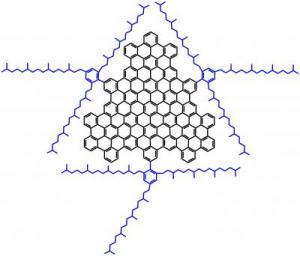
To make large sheets of carbon available for light collection, Indiana University Bloomington chemists have devised an unusual solution -- attach what amounts to a 3-D bramble patch to each side of the carbon sheet. Using that method, the scientists say they were able to dissolve sheets containing as many as 168 carbon atoms, a first.
2-D view of a graphene sheet (black) and attached sidegroups (blue)
This is a 2-D view of a graphene sheet (black)and 
attached sidegroups (blue) that IU Bloomington 
chemist Liang-shi Li and his collaborators devised. 
In reality, each sidegroup rotates 90 degrees or 
so out of graphene's plane. The three blue, tail-like 
hydrocarbons of each sidegroup have great freedom 
of movement, but two are likely to hover over the 
graphene, making it very unlikely that one 
graphene sheet will touch another. 
(Credit: Image by Liang-shi Li)

The scientists' report, online April 9, will appear in a future issue of Nano Letters.

"Our interest stems from wanting to find an alternative, readily available material that can efficiently absorb sunlight," said chemist Liang-shi Li, who led the research. "At the moment the most common materials for absorbing light in solar cells are silicon and compounds containing ruthenium. Each has disadvantages."

Their main disadvantage is cost and long-term availability. Ruthenium-based solar cells can potentially be cheaper than silicon-based ones, but ruthenium is a rare metal on Earth, as rare as platinum, and will run out quickly when the demand increases.

Carbon is cheap and abundant, and in the form of graphene, capable of absorbing a wide range of light frequencies. Graphene is essentially the same stuff as graphite (pencil lead), except graphene is a single sheet of carbon, one atom thick. Graphene shows promise as an effective, cheap-to-produce, and less toxic alternative to other materials currently used in solar cells. But it has also vexed scientists.

For a sheet of graphene to be of any use in collecting photons of light, the sheet must be big. To use the absorbed solar energy for electricity, however, the sheet can't be too big. Unfortunately, scientists find large sheets of graphene difficult to work with, and their sizes even harder to control. The bigger the graphene sheet, the stickier it is, making it more likely to attract and glom onto other graphene sheets. Multiple layers of graphene may be good for taking notes, but they also prevent electricity.

Chemists and engineers experimenting with graphene have come up with a whole host of strategies for keeping single graphene sheets separate. The most effective solution prior to the Nano Letters paper has been breaking up graphite (top-down) into sheets and wrap polymers around them to make them isolated from one another. But this makes graphene sheets with random sizes that are too large for light absorption for solar cells.

Li and his collaborators tried a different idea. By attaching a semi-rigid, semi-flexible, three-dimensional sidegroup to the sides of the graphene, they were able to keep graphene sheets as big as 168 carbon atoms from adhering to one another. With this method, they could make the graphene sheets from smaller molecules (bottom-up) so that they are uniform in size. To the scientists' knowledge, it is the biggest stable graphene sheet ever made with the bottom-up approach.

The sidegroup consists of a hexagonal carbon ring and three long, barbed tails made of carbon and hydrogen. Because the graphene sheet is rigid, the sidegroup ring is forced to rotate about 90 degrees relative to the plane of the graphene. The three brambly tails are free to whip about, but two of them will tend to enclose the graphene sheet to which they are attached.

The tails don't merely act as a cage, however. They also serve as a handle for the organic solvent so that the entire structure can be dissolved. Li and his colleagues were able to dissolve 30 mg of the species per 30 mL of solvent.

"In this paper, we found a new way to make graphene soluble," Li said. "This is just as important as the relatively large size of the graphene itself."

To test the effectiveness of their graphene light acceptor, the scientists constructed rudimentary solar cells using titanium dioxide as an electron acceptor. The scientists were able to achieve a 200-microampere-per-square-cm current density and an open-circuit voltage of 0.48 volts. The graphene sheets absorbed a significant amount of light in the visible to near-infrared range (200 to 900 nm or so) with peak absorption occurring at 591 nm.

The scientists are in the process of redesigning the graphene sheets with sticky ends that bind to titanium dioxide, which will improve the efficiency of the solar cells.

"Harvesting energy from the sun is a prerequisite step," Li said. "How to turn the energy into electricity is the next. We think we have a good start."

PhD students Xin Yan and Xiao Cui and postdoctoral fellow Binsong Li also contributed to this research. It was funded by grants from the National Science Foundation and the American Chemical Society Petroleum Research Fund.
Reblog this post [with Zemanta]