BTemplates.com

Powered by Blogger.

Pageviews past week

Quantum mechanics

Auto News

artificial intelligence

About Me

Recommend us on Google!

Information Technology

Popular Posts

Showing posts with label IBM. Show all posts

Wednesday, November 16, 2011

Mimicking the Brain -- In Silicon: New Computer Chip Models How Neurons Communicate With Each Other at Synapses


For decades, scientists have dreamed of building computer systems that could replicate the human BRAIN's talent for learning new tasks.


Researchers have taken a major step toward that goal by designing a computer chip that mimics how the brain's neurons adapt in response to new information. (Credit: MIT)

MIT researchers have now taken a major step toward that goal by designing a computer chip that mimics how the brain's neurons adapt in response to new information. This phenomenon, known as plasticity, is believed to underlie many brain functions, including learning and memory.

With about 400 transistors, the silicon chip can simulate the activity of a single brain synapse -- a connection between two neurons that allows information to flow from one to the other. The researchers anticipate this chip will help neuroscientists learn much more about how the brain works, and could also be used in neural prosthetic devices such as artificial retinas, says Chi-Sang Poon, a principal research scientist in the Harvard-MIT Division of Health Sciences and Technology.

Poon is the senior author of a paper describing the chip in the Proceedings of the National Academy of Sciences the week of Nov. 14. Guy Rachmuth, a former postdoc in Poon's lab, is lead author of the paper. Other authors are Mark Bear, the Picower Professor of Neuroscience at MIT, and Harel Shouval of the University of Texas Medical School.

Modeling synapses

There are about 100 billion neurons in the brain, each of which forms synapses with many other neurons. A synapse is the gap between two neurons (known as the presynaptic and postsynaptic neurons). The presynaptic neuron releases neurotransmitters, such as glutamate and GABA, which bind to receptors on the postsynaptic cell membrane, activating ion channels. Opening and closing those channels changes the cell's electrical potential. If the potential changes dramatically enough, the cell fires an electrical impulse called an action potential.

All of this synaptic activity depends on the ion channels, which control the flow of charged atoms such as sodium, potassium and calcium. Those channels are also key to two processes known as long-term potentiation (LTP) and long-term depression (LTD), which strengthen and weaken synapses, respectively.

The MIT researchers designed their computer chip so that the transistors could mimic the activity of different ion channels. While most chips operate in a binary, on/off mode, current flows through the transistors on the new brain chip in analog, not digital, fashion. A gradient of electrical potential drives current to flow through the transistors just as ions flow through ion channels in a cell.

"We can tweak the parameters of the circuit to match specific ion channels," Poon says. "We now have a way to capture each and every ionic process that's going on in a neuron."

Previously, researchers had built circuits that could simulate the firing of an action potential, but not all of the circumstances that produce the potentials. "If you really want to mimic brain function realistically, you have to do more than just spiking. You have to capture the intracellular processes that are ion channel-based," Poon says.

The new chip represents a "significant advance in the efforts to incorporate what we know about the biology of neurons and synaptic plasticity onto CMOS [complementary metal-oxide-semiconductor] chips," says Dean Buonomano, a professor of neurobiology at the University of California at Los Angeles, adding that "the level of biological realism is impressive.

The MIT researchers plan to use their chip to build systems to model specific neural functions, such as the visual processing system. Such systems could be much faster than digital computers. Even on high-capacity computer systems, it takes hours or days to simulate a simple brain circuit. With the analog chip system, the simulation is even faster than the biological system itself.

Another potential application is building chips that can interface with biological systems. This could be useful in enabling communication between neural prosthetic devices such as artificial retinas and the brain. Further down the road, these chips could also become building blocks for artificial intelligence devices, Poon says.

Debate resolved

The MIT researchers have already used their chip to propose a resolution to a longstanding debate over how LTD occurs.

One theory holds that LTD and LTP depend on the frequency of action potentials stimulated in the postsynaptic cell, while a more recent theory suggests that they depend on the timing of the action potentials' arrival at the synapse.

Both require the involvement of ion channels known as NMDA receptors, which detect postsynaptic activation. Recently, it has been theorized that both models could be unified if there were a second type of receptor involved in detecting that activity. One candidate for that second receptor is the endo-cannabinoid receptor.

Endo-cannabinoids, similar in structure to marijuana, are produced in the brain and are involved in many functions, including appetite, pain sensation and memory. Some neuroscientists had theorized that endo-cannabinoids produced in the postsynaptic cell are released into the synapse, where they activate presynaptic endo-cannabinoid receptors. If NMDA receptors are active at the same time, LTD occurs.

When the researchers included on their chip transistors that model endo-cannabinoid receptors, they were able to accurately simulate both LTD and LTP. Although previous experiments supported this theory, until now, "nobody had put all this together and demonstrated computationally that indeed this works, and this is how it works," Poon says.

Thursday, June 30, 2011

IBM scientists demonstrate computer memory breakthrough


For the first time, scientists at IBM Research have demonstrated that a relatively new memory technology, known as phase-change memory (PCM), can reliably store multiple data bits per cell over extended periods of time. This significant improvement advances the development of low-cost, faster and more durable memory applications for consumer devices, including mobile phones and cloud storage, as well as high-performance applications, such as enterprise data storage.

With a combination of speed, endurance, non-volatility and density, PCM can enable a paradigm shift for enterprise IT and storage systems within the next five years. Scientists have long been searching for a universal, non-volatile memory technology with far superior performance than flash – today’s most ubiquitous non-volatile memory technology. The benefits of such a memory technology would allow computers and servers to boot instantaneously and significantly enhance the overall performance of IT systems. A promising contender is PCM that can write and retrieve data 100 times faster than flash, enable high storage capacities and not lose data when the power is turned off. Unlike flash, PCM is also very durable and can endure at least 10 million write cycles, compared to current enterprise-class flash at 30,000 cycles or consumer-class flash at 3,000 cycles. While 3,000 cycles will out live many consumer devices, 30,000 cycles are orders of magnitude too low to be suitable for enterprise applications (see chart for comparisons).

“As organizations and consumers increasingly embrace cloud-computing models and services, whereby most of the data is stored and processed in the cloud, ever more powerful and efficient, yet affordable storage technologies are needed,” states Dr. Haris Pozidis, Manager of Memory and Probe Technologies at IBM Research – Zurich. “By demonstrating a multi-bit phase-change memory technology which achieves for the first time reliability levels akin to those required for enterprise applications, we made a big step towards enabling practical memory devices based on multi-bit PCM.”

Multi-level Phase Change Memory Breakthrough

To achieve this breakthrough demonstration, IBM scientists in Zurich used advanced modulation coding techniques to mitigate the problem of short-term drift in multi-bit PCM, which causes the stored resistance levels to shift over time, which in turn creates read errors. Up to now, reliable retention of data has only been shown for single bit-per-cell PCM, whereas no such results on multi-bit PCM have been reported.

PCM leverages the resistance change that occurs in the material — an alloy of various elements — when it changes its phase from crystalline — featuring low resistance — to amorphous — featuring high resistance — to store data bits. In a PCM cell, where a phase-change material is deposited between a top and a bottom electrode, phase change can controllably be induced by applying voltage or current pulses of different strengths. These heat up the material and when distinct temperature thresholds are reached cause the material to change from crystalline to amorphous or vice versa.

In addition, depending on the voltage, more or less material between the electrodes will undergo a phase change, which directly affects the cell's resistance. Scientists exploit that aspect to store not only one bit, but multiple bits per cell. In the present work, IBM scientists used four distinct resistance levels to store the bit combinations “00”, “01” 10” and “11”.


To achieve the demonstrated reliability, crucial technical advancements in the “read” and “write” process were necessary. The scientists implemented an iterative “write” process to overcome deviations in the resistance due to inherent variability in the memory cells and the phase-change materials: “We apply a voltage pulse based on the deviation from the desired level and then measure the resistance. If the desired level of resistance is not achieved, we apply another voltage pulse and measure again — until we achieve the exact level,” explains Pozidis.

Despite using the iterative process, the scientists achieved a worst-case write latency of about 10 microseconds, which represents a 100× performance increase over even the most advanced Flash memory on the market today.

For demonstrating reliable read-out of data bits, the scientists needed to tackle the problem of resistance drift. Because of structural relaxation of the atoms in the amorphous state, the resistance increases over time after the phase change, eventually causing errors in the read-out. To overcome that issue, the IBM scientists applied an advanced modulation coding technique that is inherently drift-tolerant. The modulation coding technique is based on the fact that, on average, the relative order of programmed cells with different resistance levels does not change due to drift.

Using that technique, the IBM scientists were able to mitigate drift and demonstrate long- term retention of bits stored in a subarray of 200,000 cells of their PCM test chip, fabricated in 90-nanometer CMOS technology. The PCM test chip was designed and fabricated by scientists and engineers located in Burlington, Vermont; Yorktown Heights, New York and in Zurich. This retention experiment has been under way for more than five months, indicating that multi-bit PCM can achieve a level of reliability that is suitable for practical applications.

The PCM research project at IBM Research – Zurich will continue to be studied at the recently opened Binnig and Rohrer Nanotechnology Center. The center, which is jointly operated by IBM and ETH Zurich as part of a strategic partnership in nanosciences, offers a cutting-edge infrastructure, including a large cleanroom for micro- and nanofabrication as well as six “noise-free” labs, especially shielded laboratories for highly sensitive experiments.

A History of Pioneering Memory Technology

In 1966, IBM Fellow, Dr. Robert Dennard invented dynamic random access memory — DRAM — which, when combined with the first low-cost microprocessors, opened the door to small personal computers. Today, every PC, notebook computer, game console and other computing device is loaded with DRAM chips. DRAM also powers mainframes, data center servers and most of the machines that run the Internet. In 1988, Dennard was awarded the US National Medal of Technology for the invention of DRAM. As IBM celebrates its Centennial this year, the company celebrates DRAM as one of its 100 greatest innovations.

More information: The paper “Drift-tolerant Multilevel Phase-Change Memory” by N. Papandreou, H. Pozidis, T. Mittelholzer, G.F. Close, M. Breitwisch, C. Lam and E. Eleftheriou, was recently presented by Haris Pozidis at the 3rd IEEE International Memory Workshop in Monterey, CA.

Provided by IBM

Thursday, September 2, 2010

Silicon Oxide Circuits Break BarrierNanocrystal Conductors Could Lead to Massive, Robust 3-D Storage


Rice University scientists have created the first two-terminal memory chips that use only silicon, one of the most common substances on the planet, in a way that should be easily adaptable to nanoelectronic manufacturing techniques and promises to extend the limits of miniaturization subject to Moore's Law.
Image
A 1k silicon oxide memory has been assembled by Rice and a commercial partner as a proof-of-concept. Silicon nanowire forms when charge is pumped through the silicon oxide, creating a two-terminal resistive switch. (Credit: Images courtesy Jun Yao/Rice University)

Last year, researchers in the lab of Rice Professor James Tour showed how electrical current could repeatedly break and reconnect 10-nanometer strips of graphite, a form of carbon, to create a robust, reliable memory "bit." At the time, they didn't fully understand why it worked so well.

Now, they do. A new collaboration by the Rice labs of professors Tour, Douglas Natelson and Lin Zhong proved the circuit doesn't need the carbon at all.

Jun Yao, a graduate student in Tour's lab and primary author of the paper to appear in the online edition of Nano Letters, confirmed his breakthrough idea when he sandwiched a layer of silicon oxide, an insulator, between semiconducting sheets of polycrystalline silicon that served as the top and bottom electrodes.

Applying a charge to the electrodes created a conductive pathway by stripping oxygen atoms from the silicon oxide and forming a chain of nano-sized silicon crystals. Once formed, the chain can be repeatedly broken and reconnected by applying a pulse of varying voltage.

The nanocrystal wires are as small as 5 nanometers (billionths of a meter) wide, far smaller than circuitry in even the most advanced computers and electronic devices.

"The beauty of it is its simplicity," said Tour, Rice's T.T. and W.F. Chao Chair in Chemistry as well as a professor of mechanical engineering and materials science and of computer science. That, he said, will be key to the technology's scalability. Silicon oxide switches or memory locations require only two terminals, not three (as in flash memory), because the physical process doesn't require the device to hold a charge.

It also means layers of silicon-oxide memory can be stacked in tiny but capacious three-dimensional arrays. "I've been told by industry that if you're not in the 3-D memory business in four years, you're not going to be in the memory business. This is perfectly suited for that," Tour said.

Silicon-oxide memories are compatible with conventional transistor manufacturing technology, said Tour, who recently attended a workshop by the National Science Foundation and IBM on breaking the barriers to Moore's Law, which states the number of devices on a circuit doubles every 18 to 24 months.

"Manufacturers feel they can get pathways down to 10 nanometers. Flash memory is going to hit a brick wall at about 20 nanometers. But how do we get beyond that? Well, our technique is perfectly suited for sub-10-nanometer circuits," he said.

Austin tech design company PrivaTran is already bench testing a silicon-oxide chip with 1,000 memory elements built in collaboration with the Tour lab. "We're real excited about where the data is going here," said PrivaTran CEO Glenn Mortland, who is using the technology in several projects supported by the Army Research Office, National Science Foundation, Air Force Office of Scientific Research, and the Navy Space and Naval Warfare Systems Command Small Business Innovation Research (SBIR) and Small Business Technology Transfer programs.

"Our original customer funding was geared toward more high-density memories," Mortland said. "That's where most of the paying customers see this going. I think, along the way, there will be side applications in various nonvolatile configurations."

Yao had a hard time convincing his colleagues that silicon oxide alone could make a circuit. "Other group members didn't believe him," said Tour, who added that nobody recognized silicon oxide's potential, even though it's "the most-studied material in human history."

"Most people, when they saw this effect, would say, 'Oh, we had silicon-oxide breakdown,' and they throw it out," he said. "It was just sitting there waiting to be exploited."

In other words, what used to be a bug turned out to be a feature.

Yao went to the mat for his idea. He first substituted a variety of materials for graphite and found none of them changed the circuit's performance. Then he dropped the carbon and metal entirely and sandwiched silicon oxide between silicon terminals. It worked.

"It was a really difficult time for me, because people didn't believe it," Yao said. Finally, as a proof of concept, he cut a carbon nanotube to localize the switching site, sliced out a very thin piece of silicon oxide by focused ion beam and identified a nanoscale silicon pathway under a transmission electron microscope.

"This is research," Yao said. "If you do something and everyone nods their heads, then it's probably not that big. But if you do something and everyone shakes their heads, then you prove it, it could be big.

"It doesn't matter how many people don't believe it. What matters is whether it's true or not."

Silicon-oxide circuits carry all the benefits of the previously reported graphite device. They feature high on-off ratios, excellent endurance and fast switching (below 100 nanoseconds).

They will also be resistant to radiation, which should make them suitable for military and NASA applications. "It's clear there are lots of radiation-hardened uses for this technology," Mortland said.

Silicon oxide also works in reprogrammable gate arrays being built by NuPGA, a company formed last year through collaborative patents with Rice University. NuPGA's devices will assist in the design of computer circuitry based on vertical arrays of silicon oxide embedded in "vias," the holes in integrated circuits that connect layers of circuitry. Such rewritable gate arrays could drastically cut the cost of designing complex electronic devices.

Zhengzong Sun, a graduate student in Tour's lab, was co-author of the paper with Yao; Tour; Natelson, a Rice professor of physics and astronomy; and Zhong, assistant professor of electrical and computer engineering.

The David and Lucille Packard Foundation, the Texas Instruments Leadership University Fund, the National Science Foundation, PrivaTran and the Army Research Office SBIR supported the research.

Sunday, April 11, 2010

Closing in on a Carbon-Based Solar Cell


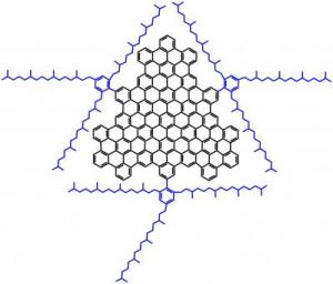
To make large sheets of carbon available for light collection, Indiana University Bloomington chemists have devised an unusual solution -- attach what amounts to a 3-D bramble patch to each side of the carbon sheet. Using that method, the scientists say they were able to dissolve sheets containing as many as 168 carbon atoms, a first.
2-D view of a graphene sheet (black) and attached sidegroups (blue)
This is a 2-D view of a graphene sheet (black)and 
attached sidegroups (blue) that IU Bloomington 
chemist Liang-shi Li and his collaborators devised. 
In reality, each sidegroup rotates 90 degrees or 
so out of graphene's plane. The three blue, tail-like 
hydrocarbons of each sidegroup have great freedom 
of movement, but two are likely to hover over the 
graphene, making it very unlikely that one 
graphene sheet will touch another. 
(Credit: Image by Liang-shi Li)

The scientists' report, online April 9, will appear in a future issue of Nano Letters.

"Our interest stems from wanting to find an alternative, readily available material that can efficiently absorb sunlight," said chemist Liang-shi Li, who led the research. "At the moment the most common materials for absorbing light in solar cells are silicon and compounds containing ruthenium. Each has disadvantages."

Their main disadvantage is cost and long-term availability. Ruthenium-based solar cells can potentially be cheaper than silicon-based ones, but ruthenium is a rare metal on Earth, as rare as platinum, and will run out quickly when the demand increases.

Carbon is cheap and abundant, and in the form of graphene, capable of absorbing a wide range of light frequencies. Graphene is essentially the same stuff as graphite (pencil lead), except graphene is a single sheet of carbon, one atom thick. Graphene shows promise as an effective, cheap-to-produce, and less toxic alternative to other materials currently used in solar cells. But it has also vexed scientists.

For a sheet of graphene to be of any use in collecting photons of light, the sheet must be big. To use the absorbed solar energy for electricity, however, the sheet can't be too big. Unfortunately, scientists find large sheets of graphene difficult to work with, and their sizes even harder to control. The bigger the graphene sheet, the stickier it is, making it more likely to attract and glom onto other graphene sheets. Multiple layers of graphene may be good for taking notes, but they also prevent electricity.

Chemists and engineers experimenting with graphene have come up with a whole host of strategies for keeping single graphene sheets separate. The most effective solution prior to the Nano Letters paper has been breaking up graphite (top-down) into sheets and wrap polymers around them to make them isolated from one another. But this makes graphene sheets with random sizes that are too large for light absorption for solar cells.

Li and his collaborators tried a different idea. By attaching a semi-rigid, semi-flexible, three-dimensional sidegroup to the sides of the graphene, they were able to keep graphene sheets as big as 168 carbon atoms from adhering to one another. With this method, they could make the graphene sheets from smaller molecules (bottom-up) so that they are uniform in size. To the scientists' knowledge, it is the biggest stable graphene sheet ever made with the bottom-up approach.

The sidegroup consists of a hexagonal carbon ring and three long, barbed tails made of carbon and hydrogen. Because the graphene sheet is rigid, the sidegroup ring is forced to rotate about 90 degrees relative to the plane of the graphene. The three brambly tails are free to whip about, but two of them will tend to enclose the graphene sheet to which they are attached.

The tails don't merely act as a cage, however. They also serve as a handle for the organic solvent so that the entire structure can be dissolved. Li and his colleagues were able to dissolve 30 mg of the species per 30 mL of solvent.

"In this paper, we found a new way to make graphene soluble," Li said. "This is just as important as the relatively large size of the graphene itself."

To test the effectiveness of their graphene light acceptor, the scientists constructed rudimentary solar cells using titanium dioxide as an electron acceptor. The scientists were able to achieve a 200-microampere-per-square-cm current density and an open-circuit voltage of 0.48 volts. The graphene sheets absorbed a significant amount of light in the visible to near-infrared range (200 to 900 nm or so) with peak absorption occurring at 591 nm.

The scientists are in the process of redesigning the graphene sheets with sticky ends that bind to titanium dioxide, which will improve the efficiency of the solar cells.

"Harvesting energy from the sun is a prerequisite step," Li said. "How to turn the energy into electricity is the next. We think we have a good start."

PhD students Xin Yan and Xiao Cui and postdoctoral fellow Binsong Li also contributed to this research. It was funded by grants from the National Science Foundation and the American Chemical Society Petroleum Research Fund.
Reblog this post [with Zemanta]

Wednesday, February 25, 2009

Work or play?


With video games gaining popularity as effective teaching tools, computer giant IBM has now devised a free game called Innov8 meant for budding businessmen

A student controls her virtual
avatar in the new Innov8 game


Computing giant IBM recently announced Innov8 v.2 – a “serious game” that helps students and professionals hone their business and technology skills in a compelling, familiar video game format.

Serious games are at the cusp of widespread adoption within all sectors of business and government, from military flight simulators to corporate training. According to leading video game marketing consultancy The Apply Group, by 2012, between 100 and 135 of the Global Fortune 500 will have adopted gaming for learning.

Innov8 v.2, IBM says, will be available at no cost to businesses and academic institutions for simulations and training.

The game features puzzles and tasks that challenge players to tackle real-world challenges; complete with a global collaboration feature for players to work with virtual teammates in order to progress to the next level of the game.

“Business simulations allow companies to optimise costs, mitigate risks and remain agile in a rapidly changing environment,” said Sandy Carter, IBM vice president of SOA (Service Oriented Architecture) and BPM (Business Process Management). “The features in this game provide a powerful tool for businesses to simulate challenges and explore the range of solutions…”

For example, Innov8 has incorporated scenarios that reflect a new level of intelligence required for future, high-value job opportunities:

•   ‘Green’ Supply Chain: Players evaluate a traditional supply chain model and are tasked with reducing a fictional company’s carbon footprint.

•   Efficient Traffic Flow: Players evaluate existing traffic patterns and re-route traffic based on sensors that alert the player to disruptions such as accidents and roadway congestion.

•   Call Centre Customer Service: Using a call centre environment, players can develop more efficient ways in which to respond to customers.

Learning Through Visualisation

“Most MBA programmess today are already heavily based on projects that reflect how individuals and teams need to interact in the real world,” Carter said. “Innov8 takes that a step further by actually allowing students to step into a dynamic business environment.”

At present, more than 100 universities – from Duquesne University and the University of Southern California in the USA, to Manchester Business School in the UK – have teamed with IBM to integrate Innov8 into their curricula.

“Until now, some of the most important skills such as leadership, project management, innovation and entrepreneurship could only be taught using standard case studies and inspirational quotes,” said Clark Aldrich, author of The Complete Guide to Simulations and Serious Games…

“IBM’s game is one way that universities can help students to learn this by doing it through simulations, in conjunction with traditional teaching methods; thus building skills and retaining knowledge,” he said.

Innov8 v.2 will be available in May 2009. For details, visit www.ibm.com/Innov8
.

Reblog this post [with Zemanta]